Normally an N-bit adder circuit is implemented using N parallel full adder circuits, simply connected next to each other. The advantage of this is that, the circuit is simple to design and purely combinatorial.
Another way to design an adder, would be to use just one full adder circuit with a flipflop at the carry output. The circuit is sequential with a reset and clock input. In each clock cycle, one bit from each operand is passed to the full adder, and the carry output is fed back as the carry input for the next SUM calculation.

The above block diagram shows how a serial adder can be implemented. The D flipflop is used to pass the output carry, back to the full adder with a clock cycle delay.
In this post, I have used a similar idea to implement the serial adder. Though I have used behavioral level approach to write my code, it should be straight forward to understand if you have the basics right.
Verilog CODE:
//serial adder for N bits. Note that we dont have to mention N here.
module serial_adder
( input clk,reset, //clock and reset
input a,b,cin, //note that cin is used for only first iteration.
output reg s,cout //note that s comes out at every clock cycle and cout is valid only for last clock cycle.
);
reg c,flag;
always@(posedge clk or posedge reset)
begin
if(reset == 1) begin //active high reset
s = 0;
cout = c;
flag = 0;
end else begin
if(flag == 0) begin
c = cin; //on first iteration after reset, assign cin to c.
flag = 1; //then make flag 1, so that this if statement isnt executed any more.
end
cout = 0;
s = a ^ b ^ c; //SUM
c = (a & b) | (c & b) | (a & c); //CARRY
end
end
endmodule
TESTBENCH CODE:
module tb;
// Inputs
reg clk;
reg reset;
reg a;
reg b;
reg cin;
// Outputs
wire s;
wire cout;
// Instantiate the Unit Under Test (UUT)
serial_adder uut (
.clk(clk),
.reset(reset),
.a(a),
.b(b),
.cin(cin),
.s(s),
.cout(cout)
);
//generate clock with 10 ns clock period.
always
#5 clk = ~clk;
initial begin
// Initialize Inputs
clk = 1;
reset = 0;
a = 0;
b = 0;
cin = 0;
reset = 1;
#20;
reset = 0;
//add two 4 bit numbers, 1111 + 1101 = 11101
a = 1; b = 1; cin = 1; #10;
a = 1; b = 0; cin = 0; #10;
a = 1; b = 1; cin = 0; #10;
a = 1; b = 1; cin = 0; #10;
reset = 1;
#10;
reset = 0;
//add two 5 bit numbers, 11011 + 10001 = 101101
a = 1; b = 1; cin = 1; #10;
a = 1; b = 0; cin = 0; #10;
a = 0; b = 0; cin = 0; #10;
a = 1; b = 0; cin = 0; #10;
a = 1; b = 1; cin = 0; #10;
reset = 1;
#10;
end
endmodule
Note that, even though this code works as a N-bit adder, we don't have to mention the value of N directly. The design keeps adding the input bits in a serial way , when the reset is not high. And in each clock cycle we get the corresponding bit on output s. The cin bit is considered to be valid only on the first clock cycle after a low reset. And the cout output bit is considered to be valid only on the first clock cycle after a high reset. After a pair of numbers are added, just apply reset for at least one clock cycle to show the end of inputs.
This way we can add binary numbers of any size without mentioning the value of N specifically.
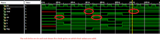
See the simulation waveform below to understand what I just explained.
The code was simulated and synthesised using Xilinx ISE 14.6 tool. You can also see a VHDL version of the same design here.
Another way to design an adder, would be to use just one full adder circuit with a flipflop at the carry output. The circuit is sequential with a reset and clock input. In each clock cycle, one bit from each operand is passed to the full adder, and the carry output is fed back as the carry input for the next SUM calculation.

The above block diagram shows how a serial adder can be implemented. The D flipflop is used to pass the output carry, back to the full adder with a clock cycle delay.
In this post, I have used a similar idea to implement the serial adder. Though I have used behavioral level approach to write my code, it should be straight forward to understand if you have the basics right.
Verilog CODE:
//serial adder for N bits. Note that we dont have to mention N here.
module serial_adder
( input clk,reset, //clock and reset
input a,b,cin, //note that cin is used for only first iteration.
output reg s,cout //note that s comes out at every clock cycle and cout is valid only for last clock cycle.
);
reg c,flag;
always@(posedge clk or posedge reset)
begin
if(reset == 1) begin //active high reset
s = 0;
cout = c;
flag = 0;
end else begin
if(flag == 0) begin
c = cin; //on first iteration after reset, assign cin to c.
flag = 1; //then make flag 1, so that this if statement isnt executed any more.
end
cout = 0;
s = a ^ b ^ c; //SUM
c = (a & b) | (c & b) | (a & c); //CARRY
end
end
endmodule
TESTBENCH CODE:
module tb;
// Inputs
reg clk;
reg reset;
reg a;
reg b;
reg cin;
// Outputs
wire s;
wire cout;
// Instantiate the Unit Under Test (UUT)
serial_adder uut (
.clk(clk),
.reset(reset),
.a(a),
.b(b),
.cin(cin),
.s(s),
.cout(cout)
);
//generate clock with 10 ns clock period.
always
#5 clk = ~clk;
initial begin
// Initialize Inputs
clk = 1;
reset = 0;
a = 0;
b = 0;
cin = 0;
reset = 1;
#20;
reset = 0;
//add two 4 bit numbers, 1111 + 1101 = 11101
a = 1; b = 1; cin = 1; #10;
a = 1; b = 0; cin = 0; #10;
a = 1; b = 1; cin = 0; #10;
a = 1; b = 1; cin = 0; #10;
reset = 1;
#10;
reset = 0;
//add two 5 bit numbers, 11011 + 10001 = 101101
a = 1; b = 1; cin = 1; #10;
a = 1; b = 0; cin = 0; #10;
a = 0; b = 0; cin = 0; #10;
a = 1; b = 0; cin = 0; #10;
a = 1; b = 1; cin = 0; #10;
reset = 1;
#10;
end
endmodule
Note that, even though this code works as a N-bit adder, we don't have to mention the value of N directly. The design keeps adding the input bits in a serial way , when the reset is not high. And in each clock cycle we get the corresponding bit on output s. The cin bit is considered to be valid only on the first clock cycle after a low reset. And the cout output bit is considered to be valid only on the first clock cycle after a high reset. After a pair of numbers are added, just apply reset for at least one clock cycle to show the end of inputs.
This way we can add binary numbers of any size without mentioning the value of N specifically.
See the simulation waveform below to understand what I just explained.

The code was simulated and synthesised using Xilinx ISE 14.6 tool. You can also see a VHDL version of the same design here.
No comments:
Post a Comment