Verilog Coding Tips and Tricks: structural level
Showing posts with label structural level. Show all posts

Monday, December 14, 2020

Synthesizable Polynomial Equation Calculator in Verilog

      A polynomial equation is an equation which is formed with variables, coefficients and exponents. They can be written in the following format:

                        y =anxn + an-1xn-1 + ... +a1x + a0 .

Here an, an-1  ... , a1 ,a0  are coefficients,

n, n-1, ... etc are exponents and x is the variable. 

In this post, I want to share, Verilog code for computing the value of 'y' if you know the value of 'x' and coefficients forming the polynomial. 

Directly calculating the polynomial with the above equation is very inefficient. So, first we reformat the equation as per Horner's rule:

                        y =(((anx + an-1)x + an-2)x + an-3)x + ... )x +a0 .

This modified equation can be represented by the following block diagram:


There are 3 sub-modules in the above block diagram.

1) Block number 1:

    This block keep generating successive powers of input x. 

In the first clock cycle it generates x^0 = 1.

In the 2ndclock cycle it generates x^1.

In the 3rd clock cycle it generates x^2.

In the nth clock cycle it generates x^(n-1).

    Every clock cycle, the previous outputs are multiplied with 'x' to get the next power of x.

2)Block number 2:

    The powers of x generated in the first block are multiplied with the corresponding coefficients of the polynomial in Block numbered 2. The coefficients are declared and initialized in the top level entity and can be changed easily.

3)Block number 4:

    This block is basically an accumulative adder which accumulates all the products generated by the multiplier. Once it does 'n' additions, we have the final result available in output 'y'. An output 'done' is set as high to indicate that the output is ready.


Let me share the Verilog codes for these modules along with the testbench.

1) power_module.v


//This module generates successive powers of input x in each clock cycle.
//For example 1,x,x^2,x^3,x^4 etc. 
//The output from the previous cycle is multiplied again by x to get the next power.
//The output from this entity is passed to the multiplier module, where it gets
//multiplied by the corresponding coefficient.
module power_module
    #(parameter N = 32)
    (   input Clock,
        input reset,
        input signed [N-1:0x,
        output signed [N-1:0] x_powered
    );

    reg signed [N-1:0] x_pow;
    reg signed [2*N-1:0] temp_prod;

    always @(posedge Clock or posedge reset ) 
    begin
        if(reset == 1)  //asynchronous active high reset.
            x_pow = 1;
        else begin
            temp_prod = x*x_pow;
            //The MSB half of the result is ignored. We assume that all intermediate powers of x
            //can be represented by a max of N bits.
            x_pow = temp_prod[N-1:0];
        end    
    end

    assign x_powered = x_pow;

endmodule


2) multiplier.v


//The successive powers of x are multiplied by the corresponding coeffcients here. 
//The results are sent to the adder module which acts as an "accumulator".
module multiplier
    #(parameter N = 32)
    (   input Clock,
        input signed [N-1:0x,y,
        output reg signed [N-1:0] prod
    );

    reg signed [2*N-1:0] temp_prod;

    always @(posedge Clock) begin
        if(Clock == 1begin
            temp_prod = x*y;
            //The MSB half of the result is ignored. We assume that all intermediate numbers
            //are represented by a max of N bits.
            prod = temp_prod[N-1:0];
        end
    end

endmodule


3) adder.v


//The output from multiplier module is received by this module and accumulated to
//form the output. If the polynomial equation has a degree of 'n' then 'n' additions has to take place
//to get the final result.
module adder
    #(parameter N = 32)
    (   input Clock,reset,
        input signed [N-1:0x,
        output signed [N-1:0] sum
    );

    reg signed [N-1:0] temp_sum;

    always @(posedge Clock or posedge reset ) 
    begin
        if(reset == 1)  //asynchronous active high reset.
            temp_sum = 0;
        else begin
            temp_sum = temp_sum + x;
        end    
    end  

    assign sum = temp_sum;

endmodule


4) Top Level Entity : poly_eq_calc.v


//This is the top level module for the polynomial equation calculator.
//The power_module, multiplier and adder modules are instantiated inside this top level block.
//When the output signal done is High, the output available at the 'y' output is the result we want.
//Ignore all other values of 'y' when done is Low.
//We have assumed that all the intermediate numbers calculated to reach the final result, can be represented
//by a maximum of N bits. This simplifies the design very much.
module poly_eq_calc
    #(parameter N = 32)
    (   input Clock,
        input reset,
        input signed [N-1:0x,
        output signed [N-1:0] y,
        output reg done
    );

    wire signed [N-1:0] x_powered,product_from_mult;
    reg signed [N-1:0] coeff;
    reg reset_adder;
    integer coeff_index;
    parameter  NUM_COEFFS = 4//Change here to change the degree of the polynomial. 
    reg signed [N-1:0] Coeffs [0:NUM_COEFFS-1];
    
    //Eq : 3*x^3 - 2*x^2 - 4*x + 5;
    //The coefficients belonging to higher powers of x are stored in higher addresses in Coeffs array.
    initial begin
        Coeffs[0] = 5;
        Coeffs[1] = -4;
        Coeffs[2] = -2;
        Coeffs[3] = 3;
    end 

    //Instantiate the 3 sub-modules.    
    power_module #(.N(N)) calc_power_of_x
        (Clock,reset,x,x_powered);

    multiplier #(.N(N)) multiply 
        (Clock,x_powered,coeff,product_from_mult);

    adder #(.N(N)) add  
        (Clock,reset_adder,product_from_mult,y);

    //The Always block controlling the 3 sub-modules and also supplying them with coefficients.   
    always @(posedge Clock or posedge reset ) 
    begin
        if(reset == 1begin    //asynchronous active high reset.
            done = 0;
            coeff_index = 0;
            coeff = Coeffs[0];
            reset_adder = 1;
        end
        else begin
            //the disabling of 'reset of adder' gets noticed by adder entity in the next clock cycle.
            reset_adder = 0
            if(coeff_index < NUM_COEFFS-1begin
                coeff_index = coeff_index+1;
                coeff = Coeffs[coeff_index];  //send the coefficients one by one to the multiplier module.
            end 
            else if(coeff_index == NUM_COEFFS-1
                coeff_index = coeff_index+1;
            else
                done = 1;    //The final result is available in 'y' now.
        end    
    end

endmodule


5) Testbench : tb_poly_eq_calc.v


//Testbench code.
module tb_poly_eq_calc;  //testbench module is always empty. No input or output ports.

    parameter Clock_period = 10;    //Change clock period here. 
    parameter N = 32;    //change the width of input and output here.
    reg Clock;
    reg reset;
    reg [N-1:0x;
    wire [N-1:0] y;
    wire done;
    integer input_num;

    //Apply inputs here. Only 'x' can be changed here.
    //To change coefficients and degree of polynomial edit the top level module directly.
    initial
    begin
        Clock = 0;
        input_num = 0;
        reset = 1;
        #(Clock_period * 2.5);
        reset = 0;

        apply_input(4);     //first input.
        apply_input(7);     //second input.
        apply_input(15);     //third input.
        apply_input(-9);     //fourth input.
        #Clock_period;          //wait for one clock cycle.
        $stop;  //Stop the simulation, as we have finished testing the design.
    end

    //the verilog task for applying one input.
    task apply_input;
        input [N-1:0] x_in;
    begin
        reset = 1;
        #Clock_period;
        reset = 0;
        x = x_in;
        #Clock_period;
        wait(done);     //wait for result to be out.
        check_result(x_in);     //verify the result.
        #Clock_period;
    end
    endtask

    //Verilog task to check if the results are correct and report.
    task check_result;
        input [N-1:0] x_in;
        integer actual_res;
    begin
        wait(Clock);
        if(done == 1begin
            //Change this equation if you change the polynomial eq inside the top level module.
            actual_res = 3*x_in*x_in*x_in - 2*x_in*x_in - 4*x_in + 5;  
            input_num = input_num+1;
            if(actual_res == y) 
                $display("Input number %d Worked Well",input_num);
            else
                $display("Input number %d Has Error",input_num);                 
        end
    end
    endtask

    //generate a 50Mhz clock for testing the design.
    always #(Clock_period/2Clock <= ~Clock;

    //Instantiate the polynomial calculator.
    poly_eq_calc #(.N(N)) poly_calculator 
            (.Clock(Clock), 
            .reset(reset), 
            .x(x), 
            .y(y),
            .done(done));


endmodule   //End of testbench.


The code was simulated successfully using Modelsim 10.4a version. The simulation waveform below shows the signals for the first set of input:


Friday, December 11, 2020

Quaternary Signed Digit (QSD) Based Fast Adder In Verilog

     Quaternary Signed Digit is a base-4 number system where a number is represented by one of the following 7 digits : -3,-2,-1,0,1,2,3. The advantage of this number system is that it allows carry free addition, thus speeding up the addition process.

    Fast adders based on QSD are typical and there are several papers on this. In this post I have written Verilog code for a 4 digit(each input being 12 bits) QSD adder. With a bit of editing, this code can be extended to handle larger input numbers.

    One thing to be careful about is that while checking online for information on QSD adders, I came upon several papers with some little mistakes here and there. Even though these typos are small, but it can take hours of your debugging time, as it did in my case. So I recommend cross checking any circuit diagram you see online across several references.

The Block diagram for the design is given below:


A QSD adder has two stages. 

In the first stage we perform operation on a single digit from each operand to form an intermediate carry and sum. The carry is 2 bit and can have one of the three values from -1 to +1. 
The sum is 3 bit and can have one of the 7 values from -3 to +3.

In the second stage, the intermediate carry and sum are simply added to form a single 3 bit sum which is between -3 to +3.

For an N digit QSD adder we have two input operands each N*3 bit in size. The Carry output is 2 bit in size and Sum output is N*3 bit in size. 

For a N digit QSD adder we need N carry-sum generators and N-1 adders. How these blocks are connected together are shown in the block diagram above.

The boolean equations for these blocks are available in Page 4 of the second pdf shared in this blog. But some of these equations are not correct. But the circuit diagram given in the page 5 of the same pdf is correct and you can refer it to form the correct boolean equations.

The carry sum generator can be better understood by looking at the Table 2 and 3 of the first pdf. And table 5 gives more clarity on how the second step adder is working.

The Verilog codes are given below:

First step : Carry Sum Generator


//QSD carry sum generator.
module QSD_cs_gen(
        input [2:0] A,B,
        output [2:0] S,
        output [1:0] C);

wire [2:0] anot,bnot;
wire [2:0] ss;
wire [1:0] cc;
wire temp1,temp2,temp3,temp4;
wire temp5,temp6,temp7,temp8,temp9;

assign anot = ~A;
assign bnot = ~B;
assign temp1 = ~(A[1] | B[1]);
assign temp2 = A[2] & bnot[0];
assign temp3 = B[2] & anot[0];
assign temp4 = temp1 & (temp2 | temp3);
assign cc[1] = (A[2] & B[2] & ~(A[0] & B[0] & A[1] & B[1]) | temp4);
assign cc[0] = cc[1] | ((anot[2] & bnot[2]) & 
                        ((A[1] & B[1]) | (B[1] & B[0]) | (B[1] & A[0]) | (B[0] & A[1]) | (A[1] & A[0])));

assign ss[0] = A[0] ^ B[0];
assign ss[1] = A[1] ^ B[1] ^ (A[0] & B[0]);
assign temp5 = (ss[0] & (A[1] ^ B[1]));
assign temp6 = (B[2] & anot[1] & bnot[0]);
assign temp7 = (A[2] & bnot[1] & anot[0]);
assign temp8 = ( A[0] & B[0] & anot[1] & bnot[1] & (A[2] | B[2]) );
assign temp9 = ( A[0] & B[0] & A[1] & B[1] & A[2] & B[2] );
assign ss[2] = temp5 | temp6 | temp7 | temp8 | temp9;

//Finally assign the temperory variables into the output ports.
assign S = ss;
assign C = cc;

endmodule


Second step : Addition of Intermediate Carry and Sum


//QSD step 2: adder for adding intermediate carry & sum.
module QSD_adder(
    input [1:0] A,
    input [2:0] B,
    output [2:0] S);

wire [2:0] sum;
wire temp1,temp2,temp3,temp4;

assign sum[0] = A[0] ^ B[0];
assign sum[1] = A[1] ^ B[1] ^ (A[0] & B[0]);
assign temp1 = A[1] & B[1];
assign temp2 = A[1] ^ B[1];
assign temp3 = A[0] & B[0];
assign temp4 = temp1 | (temp2 & temp3);
assign sum[2] = A[1] ^ B[2] ^ temp4;    
    
assign S = sum;

endmodule

4 Digit QSD Adder:


//4 digit QSD adder. 
module QSDAdder(
        input [11:0] A,B,
        output [1:0] Cout,
        output [11:0] S);
 
//temperory variables 
wire [2:0] S1,S2,S3;
wire [1:0] C0,C1,C2,C3;

//First stage to QSD addition : The 4 carry-sum generators.
QSD_cs_gen carry_sum_gen1 (
        .A(A[2:0]),
        .B(B[2:0]),
        .S(S[2:0]),
        .C(C0)
        );

QSD_cs_gen carry_sum_gen2 (
        .A(A[5:3]),
        .B(B[5:3]),
        .S(S1),
        .C(C1)
        );

QSD_cs_gen carry_sum_gen3 (
        .A(A[8:6]),
        .B(B[8:6]),
        .S(S2),
        .C(C2)
        );

QSD_cs_gen carry_sum_gen4 (
        .A(A[11:9]),
        .B(B[11:9]),
        .S(S3),
        .C(Cout)
        );
 
//Second stage to QSD addition : The addition of intermediate carry's and sum's
QSD_adder adder1 (
        .A(C0),
        .B(S1),
        .S(S[5:3])
        );

QSD_adder adder2 (
        .A(C1),
        .B(S2),
        .S(S[8:6])
        ); 

QSD_adder adder3 (
        .A(C2),
        .B(S3),
        .S(S[11:9])
        );

endmodule


Testbench for the 4 Digit QSD Adder:


//Testbench code which tests all combinations of inputs to a 4 digit QSD adder
module tb_QSDAdder;

  reg [11:0] A,B;
  wire signed [1:0] Cout;
  wire [11:0] S;

    //A function to convert 12 bit QSD number to a signed integer.
    function [31:0] qsd2int;
        input [11:0] A;
        reg signed [31:0] res;
        reg signed [31:0] temp;
        integer i;
    begin
        res = 0;
        temp = 0;
        for (i = 0; i < 4; i = i + 1begin     //run the loop through all the digits.
            temp = {{29{A[2+3*i]}}, A[3*i+:3]};  //sign extension
            res = res + (temp << (2*i)); //shift left and accumulate.
        end
        qsd2int = res;
    end
    endfunction

    reg [31:0] error;

    //Instantiate the QSD based adder for testing.
    QSDAdder UUT (
      .A(A),
      .B(B),
      .Cout(Cout),
      .S(S));

    initial 
    begin
        error = 0;
        apply_inputs;
        $100;
        $display("End Of Simulation Reached. Number of Errors = %d",error);
        $stop;  //Stop running the simulation as we have tested for all variation of inputs.
    end

    //this task is where we generate inputs to apply to the adder.
    //4 digits for one number. and we have two numbers. 
    //so 8 for-loops to generate all combination of values for all digits.
    task apply_inputs;
        //the loop indices are declared as 4 bit instead of 3 bit to avoid overflow error.
        reg signed [3:0] i,j,k,l,m,n,o,p;   
    begin
        #5//wait for 5 ns;
        for(i=-3;i<=3;i=i+1begin
            for(j=-3;j<=3;j=j+1begin
                for(k=-3;k<=3;k=k+1begin
                    for(l=-3;l<=3;l=l+1begin
                        A = {i[2:0],j[2:0],k[2:0],l[2:0]};  //take LSB 3 bits to form A.
                        for(m=-3;m<=3;m=m+1begin
                            for(n=-3;n<=3;n=n+1begin
                                for(o=-3;o<=3;o=o+1begin
                                    for(p=-3;p<=3;p=p+1begin
                                        B = {m[2:0],n[2:0],o[2:0],p[2:0]};  //take LSB 3 bits to form B.
                                        #10 check_results;  //Check if the results from the module are correct.
                                    end
                                end
                            end
                        end
                    end
                end
            end
        end
    end    
    endtask


    //the outputs are checked compare with actual sum in this task.
    //A variable 'error' in incremented in case of an error.
    task check_results;
        reg signed [31:0] A_dec,B_dec,S_dec,S_dec1,S_act1;
    begin
        A_dec = qsd2int(A);     //convert QSD to decimal format
        B_dec = qsd2int(B);     //convert QSD to decimal format
        S_dec = qsd2int(S);     //convert QSD to decimal format
        //if carry out is -1 we subtract 256. or else we add 256 if carry out is 1.
        S_dec1 = S_dec + 256*Cout;
        S_act1 = A_dec+B_dec;   //Actual result.
        //if result from adder and actual sum doesnt match, increment "error"
        if(S_dec1 != S_act1)
            error = error+1;
    end
    endtask

endmodule
    

A bit of explanation on the Verilog codes:

    The first two codes, QSD_cs_gen and QSD_adder, are simply based on the boolean equations and circuit diagram presented in the second pdf. Its a gate level code. Note that I have broken the long equations into several lines by using temporary variables. This adds clarity as well as makes the code you write less prone to error.

    The third code, QSDAdder, is the 4 digit QSD adder, which connects the above two blocks in a structural level design.

    The fourth code, tb_QSDAdder, is the testbench for testing the functionality of our adder. This is relatively complicated compared to the other three blocks of code.

    Testbench has a function named qsd2int, which converts a 4 digit QSD number into a signed integer number. Each digit of the QSD number is sign extended to 32 bits and then left shifted by a multiple of 2 before accumulatively adding to the result. Left shifting here simply means I am trying to multiply by 1,4,16,64 etc. based on the index of the digit.

    In the testbench I want to test the design for all the possible combinations of inputs. There are two 4 digit QSD numbers and each number has 7 possible values.  Which means that the number of sets of inputs is 7^(4+4) = 7^8 = 5764801. This is achieved in a task named apply_inputs.

    The resultant sum from the Adder module are compared with the actual result in another task named check_results. If there is a mismatch in this comparison, a variable named error is incremented by 1. The Adder is fully working, if by the end of the simulation, error is still 0.

    Verilog codes and papers which I have referred to write the codes can be downloaded as a Zipped file from here

    Note that the Boolean equations in the second paper have some mistakes. But you can check the circuit diagram, which seems to be correct. Cross check with the Verilog codes if you are not sure. 

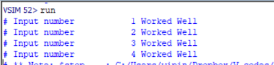
    The codes were simulated and tested successfully using Modelsim 10.4a.

Part of the simulation waveform is shown below:


The same design was implemented in VHDL, few weeks back in my other blog. You can check it out here.


Friday, November 3, 2017

Verilog code for Carry Save Adder with Testbench

Carry save adder is very useful when you have to add more than two numbers at a time. Normally if you have three numbers, the method would be to add the first two numbers together and then add the result to the third one. This causes so much delay.

In this post I have implemented a 4 bit carry save adder which adds three numbers at a time. You might want to see page 1 and 2 of this paper to get a better understanding of how this exactly works.

fulladder.v

module fulladder
        (   input a,b,cin,
            output sum,carry
            );

assign sum = a ^ b ^ cin;
assign carry = (& b) | (cin & b) | (& cin);

endmodule

CSA.v

module CSA
        (   input [3:0] x,y,z,
            output [4:0] s,
            output cout
            );
            
wire [3:0] c1,s1,c2;

fulladder fa_inst10(x[0],y[0],z[0],s1[0],c1[0]);
fulladder fa_inst11(x[1],y[1],z[1],s1[1],c1[1]);
fulladder fa_inst12(x[2],y[2],z[2],s1[2],c1[2]);
fulladder fa_inst13(x[3],y[3],z[3],s1[3],c1[3]); 

fulladder fa_inst20(s1[1],c1[0],1'b0,s[1],c2[1]);
fulladder fa_inst21(s1[2],c1[1],c2[1],s[2],c2[2]);
fulladder fa_inst22(s1[3],c1[2],c2[2],s[3],c2[3]);
fulladder fa_inst23(1'b0,c1[3],c2[3],s[4],cout); 

assign s[0] = s1[0];

endmodule

tb_adder.v

module tb_adder;

    reg [3:0] x,y,z;
    wire [4:0] s;
    wire cout;  
    integer i,j,k,error;

    // Instantiate the Unit Under Test (UUT)
    CSA uut (x,y,z,s,cout);

//Stimulus block - all the input combinations are tested here.
//the number of errors are recorded in the signal named "error".
    initial begin
        // Initialize Inputs
        x = 0;
        y = 0;
        z = 0;
        error = 0;
        //three for loops to test all input combinations.
      for(i=0;i<16;i=i+1) begin
            for(j=0;j<16;j=j+1) begin
                for(k=0;k<16;k=k+1) begin
                     x = i;
                     y = j;
                     z = k;
                     #10;
                     if({cout,s} != (i+j+k)) 
                          error <= error + 1;
                end       
            end  
      end
    end 
    
endmodule

Simulation waveform:

The simulated waveform in Xilinx ISIM would look like this: